More EE Interview Questions
Unlike some of my previous EE Interview questions, this one includes some discussion. The word “schematic” comes from the root word “scheme.” The idea is that a schematic diagram shows you the general scheme or plan for a design. Generally, a schematic diagram will include every electrical connection, but will not show you the path or physical routing of those connections. A schematic is like a skimpy swimming suit: what it shows is interesting, but what it hides is important.
I have been known to show a candidate part of a schematic diagram and then ask them what is over-simplified or misleading about that drawing. Let’s look at a really simple example.
This might be the power connection to something like a processor or memory device.
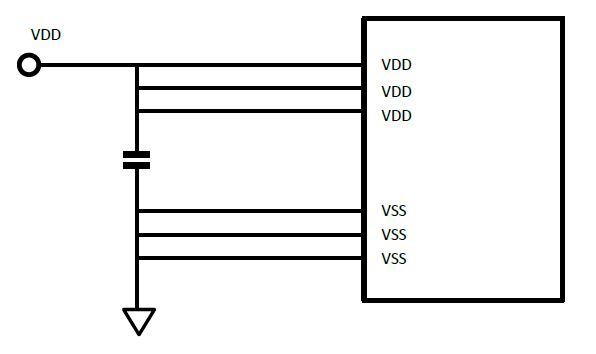
One of the responses that I am hoping to hear from the candidate is that the connections, represented by a straight line in the schematic, most probably are not at all like the “perfect conductors” the schematic simplifies them to be.
In fact, in the physical embodiment, each of those traces on the Printed Circuit Board (PCB) will be effectively made from lots of distributed inductance, capacitance, and resistance. These differences from a non-ideal conductor contribute to unwanted signals (noise) at the pins of the device.
I might need to coach a candidate a tiny bit to get them to understand the general direction of my question. I might say, “Well, just scribble on this drawing what the connections really look like to the power flowing through them.” Most engineers would figure out where this is headed and produce something like this second sketch.
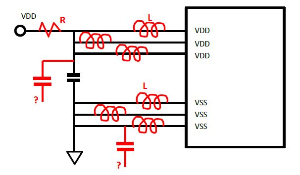
The candidate might explain that if the PCB design is really awful, there might be significant voltage drop (E=I*R) at some of the device pins. But even with a reasonable PCB layout, we might see significant switching noise at the VDD and VSS pins of the device (E = L*di/dt) due to the extremely short intervals where the P and N FETs of a CMOS device are both turned ON. A sharp engineer will tell me that even though L is very small for those connections, di/dt can be very, very large. Also, some stray capacitive coupling can exist to other nodes in the circuit.
Assuming the candidate has provided some reasonable responses to these inquiries, this follow-up question from me will quickly reveal how much experience they have in circuit board development: “How do we convey to the PCB layout engineer what he should do in the layout to get the best performance for this design?”
As with many good interview questions there is no single correct response. There are many, many good responses. Some good answers the candidate might say include:
- We provide pages of layout notes describing the general plan for the Power Delivery Network (PDN) and signal routing strategy: including the number of PCB layers, the planned PCB stackup (layer copper thickness and spacing,) bypass capacitor placement, trace width requirements for some critical traces, any trace length matching or trace spacing and length restrictions, and via counts and sizes for special layer-to-layer connections.
- We provide a copy of the silicon vendor’s reference design layout to our PCB layout engineer. This might lead to an extensive discussion if the silicon vendor’s reference design demands more layers than we can afford, or if we believe that their reference design will not deliver the performance or density of design that our implementation will require.
- We provide sketches or copies of similar critical layout areas that we have used in the past.
- After initial layout, we perform multiple schematic and PCB layout design reviews with team members and outside teams (for example with the silicon vendor’s team).
- My follow-up question: “What if the silicon vendor demands that you include something which your plan and strategy make very difficult or even impossible?”
- I hope the candidate says, “We cannot simply ignore their input, but might try to reach a compromise engineering solution.”
- My follow-up question: “What if the silicon vendor demands that you include something which your plan and strategy make very difficult or even impossible?”
The one top-level response that would make me conclude a candidate is not appropriate for our team is if they were to say, “Oh, I would just tell the layout engineer what I want.”
That answer is completely contrary to the concepts of “Write Stuff Down” or “Document or Die.” That answer shows a lack of engineering maturity. To which I might think, “Next candidate, please!”